| Manufacturing Materials | Capability |
|---|---|
| FR4 | Tg 135: KB6160, S1141 Tg 150: KB6165, S1000H Tg 170: KB6167, S1000-2M, IT180A, TU768 |
| Halogen Free FR4 | Tg 150: S1150G Tg 170: S1165, TU862HF |
| Ceramic Filling High Frequency Material | Rogers 4003C/4350B |
| PTFE High Frequency Material | Rogers Series, Arlon Series, Taconic Series, F4BM Series |
| Special PP | NFPP: Arlon 49 N, VT47 Ceramic Filling PP: Rogers 4450F PTFE PP: Arlon 6700, Taconic FR-27 |
| Rigid PI Material | Arlon 85 N, VT901 |
| Metal Base Board | Bergquist Al base, Chinese Brand Al base, Copper base |
| Material Mixed Laminate | 4 layers – 10 layers (FR4 + Ro4350, FR4 + Aluminium, FR4 + FPC) |
| Note | Other special materials can be processed and produced by means of customer supply or purchasing. |
| Item | Standard | Advanced | Innovative |
|---|---|---|---|
| IC Space (Green Color) | 4 | 4 | 3 |
| IC Space (Other Color) | 5 | 5 | 4 (blue oil) |
| Liquid Photoimageable (LPI) Solder Mask Registration | 3mil | 2mil | 1.5mil |
| Thickness T>1.0 mm | ±10% | ±10% | ±8% |
| Tolerance T≤1.0 mm | ±0.1 | ±0.1 | ±0.1 |
| Board Thickness (mm) | 0.5-5.0 | 0.4-6.5 | 0.25-10 |
| Hole Aspect Ratio | 10:01 | 12:01 | 20:01 |
| Via Size For Plug Solder Mask | 0.25-0.5 | 0.20-0.5 | 0.15-0.6 |
| Via Size For Plug Resin And Capped Copper | 0.25-0.5 | 0.20-0.5 | 0.075-0.6 |
| Panel Size (mm) | 457×609 | 457×609 | 600×1000 |
| Bow And Twist | ≤0.75% | ≤0.75% | ≤0.5% |
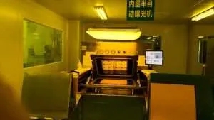
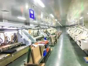
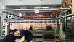
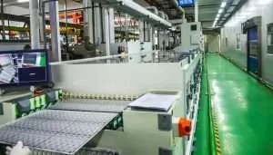
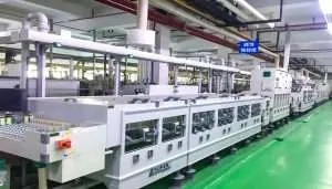
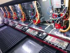 Step 7: Hole Drilling